PDP-8/I · Volume 6
PDP-8/I — Volume 6 — Core Memory & the Physical Machine
Ten thousand ferrite rings threaded by hand, a hundred plug-in cards on a wire-wrapped backplane, and a wall of switches and lamps — the actual object the architecture had to be carved into out of magnetism, silicon, and sheet metal.
6.1 About This Volume
Volumes 4 and 5 took apart the architecture of the PDP-8/I — the twelve-bit word, the field carved into pages, the single accumulator, the instruction set built on top of them. That was the abstract machine, the one a programmer holds in mind. But the abstract machine has to live somewhere. Twelve-bit words have to be stored in some physical stuff that remembers them; the logic that fetches and adds and rotates them has to be built out of some real components; and the whole thing has to be bolted into a box, fed power, kept cool, and given a face an operator can touch. This volume is about that physical machine — the real object on the bench, the thing Jeff’s replica reaches back to evoke.
It is the most concrete volume in the series. Where Volume 4 dealt in registers you cannot see and Volume 5 in addressing modes that exist only as patterns of bits, this one is about ferrite and copper and printed-circuit board. We start with the strangest and most beautiful part — the magnetic-core memory, a fabric of tiny iron rings threaded with wire, each ring remembering one bit by the direction it is magnetized — and see why reading such a memory destroys what it reads. We then climb into the logic: the small TTL integrated circuits of the late 1960s, mounted on DEC’s M-series flip-chip cards, tied together by a wire-wrapped backplane. And finally we tour the whole assembled object — core stack, module rows, backplane, power supply, and the front panel of switches and lamps. The operation of that panel — how you toggle a program in by hand — is the subject of Volume 7; here the panel is just hardware, one more physical thing in the box.
6.2 How magnetic-core memory works
The memory of a PDP-8/I is not made of chips. In 1968 the integrated-circuit memory that would later become universal did not yet exist in any practical, affordable form, and a computer’s main store was built instead from magnetic-core memory — a technology so unlike anything in a modern machine that it is worth describing from first principles, because once you see how it works you understand a great deal about why the PDP-8 behaves as it does.
The storage element is a core: a tiny ring, or toroid, of ferrite — a hard, ceramic-like magnetic material — about thirty-five thousandths of an inch across, smaller than a grain of rice, with a hole finer than the lead of a pencil. Each ring stores exactly one bit, by being magnetized in one of two directions around its circumference: the magnetic field can circulate clockwise or counter-clockwise, and those two directions stand for a 0 and a 1. Nothing about the ring moves; what is stored is purely the direction of its magnetization, frozen into the iron.
What makes a ferrite ring usable as a memory cell — rather than just a magnet that gradually forgets — is a property of the material called hysteresis. Plot how strongly the ring is magnetized against the field you apply to it, and the curve does not run straight through the origin; it traces a wide, squarish loop. The practical meaning is this: the ring has two stable states, fully magnetized one way and fully magnetized the other, and it stays in whichever one it is in. A small applied field nudges it nowhere. Only a field stronger than a definite threshold will force it across to the other state, where it then sits just as stubbornly. The ferrite, in other words, is bistable: two settled positions with a wall between them, and it remembers which side of the wall it is on. That squareness of the hysteresis loop — the sharp threshold, the firm memory — is the whole reason cores work, and choosing ferrite formulations with the squarest possible loops was a serious materials-science craft of the era.
Now the problem: a working memory needs thousands of these rings, and you cannot run a private pair of control wires to every one — the wiring would dwarf the memory. DEC’s PDP-8/I core, like all the core memory of its generation, solves this with a beautifully economical trick called coincident-current selection, and it is the single most elegant idea in the whole technology. The cores are arranged in a flat square grid, and two sets of wires are threaded through them: a set of horizontal wires (call them the X lines), one per row, and a set of vertical wires (the Y lines), one per column. Every core sits at the crossing of exactly one X wire and one Y wire, threaded by both.
The trick lies in the threshold. To flip a core you need a current strong enough to push its magnetization over the hysteresis wall — call that the full select current. But you never send a full current down any wire. Instead you send half of it down the one X wire and half down the one Y wire whose crossing point is the core you want. At every other core on that X wire, only half a current is present — not enough to flip anything; at every other core on that Y wire, likewise only half. But at the one core where the chosen X and Y wires cross, the two half-currents add together, and only there does the total reach the full select current that drives the ring over its threshold. Two half-currents, summing at exactly one intersection in a grid of thousands — that single core flips, and no other is disturbed. With nothing more than one wire per row and one per column, any ring in the grid can be singled out. The squareness of the hysteresis loop is what makes it safe: a half-current must be reliably below the flip threshold while two together are reliably above it.
Selecting a core is only half the job; you also need to read what it holds and write a chosen value into it, and for that the PDP-8/I’s core uses two more wires, giving four through each core in all. The sense wire runs diagonally through all the cores of a plane and does the reading, exploiting a basic law of physics: when a core’s magnetization flips, that sudden change of field induces a small voltage pulse in any wire passing through the ring. So to read a core, the memory drives the X and Y half-currents in the direction that would set it to 0. If the core was already 0, nothing happens — no flip, no pulse. If it held a 1, it flips to 0, throwing a tiny pulse onto the sense wire. A sense amplifier watches for that pulse: pulse means the core had been a 1; silence means a 0. The memory reads the bit not by looking at the core’s state but by trying to clear it and noticing whether it had to.
The fourth wire is the inhibit wire, and it governs writing. Writing a 1 is just selection in the opposite direction: drive the X and Y half-currents the way that sets a 1, and the core flips to 1. But what if you want to write a 0? You cannot simply withhold the drive currents, because the X and Y lines serve a whole row and column at once — they are driving the other cores too. So the inhibit wire carries, when needed, a half-current opposing the write direction. At the one core you wish to leave at 0, that opposing half-current cancels one of the two driving half-currents, the total never reaches the flip threshold, and the core stays at 0. The inhibit line, in effect, vetoes the write at a chosen bit. Between the four wires the whole job is done: X and Y to select, sense to read out the flip, inhibit to suppress an unwanted write. Here is the threading, looking down on a corner of one plane:
        Y0          Y1          Y2          Y3      <- Y drive lines (columns)
         |           |           |           |
   X0 ---O-----------O-----------O-----------O---    <- X drive line (row)
         |\          |\          |\          |\
   X1 ---O-\---------O-\---------O-\---------O-\-
         |  \        |  \        |  \        |  \
   X2 ---O---\-------O---\-------(O)--\-------O---\   <- core (O) at X2,Y2
         |    \      |    \      | ^  \      |    \      is SELECTED:
   X3 ---O-----S-----O-----S-----O-S---S-----O-----S    half-I on X2
                                   |                     + half-I on Y2
   Each core threaded by 4 wires:  |                     = full flip current
     X  (row, half select current) |
     Y  (column, half select current)
     S  sense  (diagonal — catches the voltage pulse when a core flips)
     I  inhibit (parallel to Y — half current that VETOES an unwanted write)

   Half + half add ONLY at the chosen X/Y crossing -> one core flips.
   Every other core on those lines sees only half -> stays put.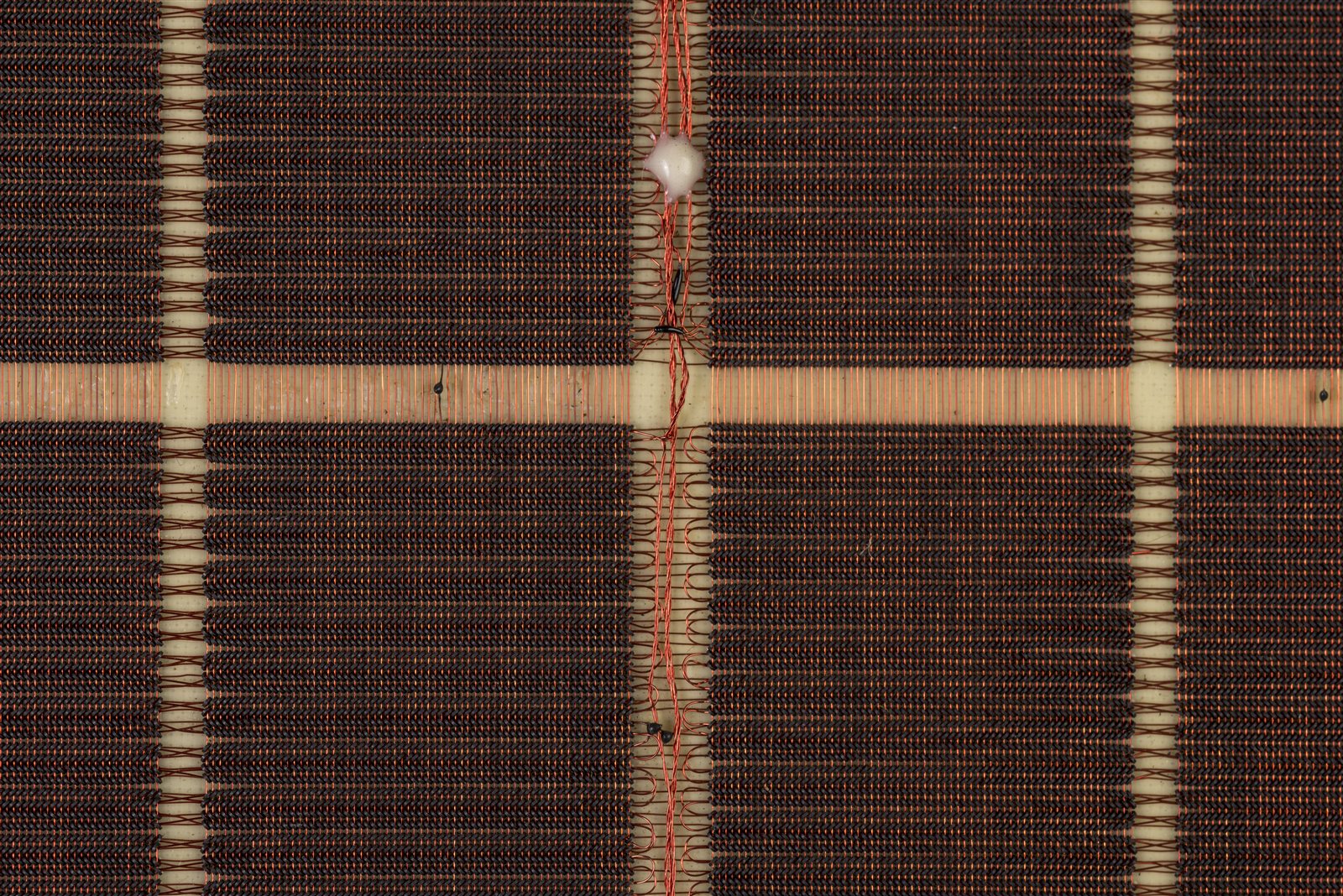
It is worth pausing on the sheer physicality of this. A core plane was woven — the rings held in a fixture and the hair-fine wires laced through their tiny holes, much of the work done by hand under magnification. A 4K plane is more than four thousand rings, each individually threaded: the memory of a PDP-8/I was, quite literally, a textile of iron and copper.
6.3 Destructive readout and the read–rewrite cycle
Look again at how reading works and a disquieting consequence falls out. To read a core, the memory tries to set it to 0 and watches for a flip — which means a core holding a 1 is left at 0 by the act of reading it. The read does not merely observe the bit; it clobbers it. This is the defining quirk of core memory, called destructive readout (DRO): every read erases what it reads, slamming the selected cores to 0 and destroying the stored word.
A memory that forgot a word the moment you looked at it would be useless, so core hides the damage by immediately putting the word back. The sense amplifiers, during the read, captured the word that was there — that is the whole point of the read. So right after the destructive read, the memory performs a write-back: it drives the cores in the set-to-1 direction and uses the inhibit lines, bit by bit, to write the captured word back into the very cores it just cleared. Seen from outside, the word survives a read unharmed — but only because the hardware quietly rewrote it. Every read of core memory is really a read followed by a restore, an indivisible two-step dance.
This is the origin of a distinction that confuses people coming from modern memory: the difference between access time and cycle time. The access time is how soon the data is available after you ask — roughly, how long the destructive read alone takes. But you cannot start another operation until the mandatory write-back has finished restoring the word. The cycle time is the full read-plus-rewrite round trip, the soonest the memory can begin its next access. For the PDP-8/I’s core that full cycle is about 1.5 microseconds — not a pure access time but a complete read-and-restore. The number is more than a curiosity: the machine’s instruction timing is built directly on the memory cycle. A simple add, which fetches the instruction in one memory cycle and the operand in another, takes about two such cycles — on the order of three microseconds. The speed of the whole machine is, at bottom, the speed of its core. (Early 8/I systems were in fact plagued by core that could not reliably hold the 1.5-microsecond pace, and some shipped detuned to a slower cycle — a reminder of how close to the edge the memory ran.)
If destructive readout is core memory’s great vice, it is balanced by a magnificent virtue: core is non-volatile. A magnetized ferrite ring keeps its magnetization with no power at all — the direction is frozen into the iron. Switch a core machine off, come back the next morning, switch it on, and the memory contents are exactly as they were left. There is no battery, no refresh, no trickle of current keeping the bits alive; the bits persist because magnetism, once set, simply stays. Modern dynamic RAM cannot do this — it forgets within fractions of a second of losing power — and core’s permanence gave the machines a robustness operators relied on: a program toggled laboriously into memory through the front panel was still there after a power cycle, and a crashed machine could often be restarted with its data intact.
6.4 The 8/I’s memory in particular
We can now assemble the abstract picture of Volume 4 — a 4K field of twelve-bit words — out of the physical cores just described. The basic PDP-8/I carries one field: 4,096 words, each twelve bits wide. The natural way to build that from cores is to give each bit position its own plane. So the memory is organized as twelve bit-planes, one for every bit of the word, and each plane is a grid of 4,096 cores — conventionally a 64-by-64 array, threaded by 64 X lines and 64 Y lines so the coincident-current scheme can address any of the 4,096 positions.
The crucial idea is how a word maps onto this stack. The planes are stacked physically one above another and wired so that the same X/Y address selects the corresponding core in every plane at once. Address location 1234 octal, and you select the core at that grid position in all twelve planes simultaneously: bit 0 of the word lives in plane 0, bit 1 in plane 1, and so on through bit 11 in plane 11. Read that address and twelve sense amplifiers, one per plane, each report their bit; together they deliver the whole twelve-bit word in parallel. Write it, and twelve inhibit lines each decide whether their bit becomes a 1 or a 0. The word is spread across the stack, one bit to a plane, and the planes act in concert — which is exactly why a 4K-by-12 memory is built as twelve planes of 4,096 cores rather than one giant grid: it lets a single coincident-current address fetch or store a whole word at once.
In the PDP-8/I the whole subsystem was a self-contained core memory module — the Type 184A — a compact assembly only an inch or so thick, built from a few rigid printed-circuit boards holding the woven core stack and packed into a small aluminum box roughly six inches across. (The bare cores would be useless alone; the module also carried supporting flip-chip cards — the X and Y drivers, the sense amplifiers, the inhibit drivers, and the address-decoding matrices that turn a twelve-bit address into the right pair of selected lines.) That little box, woven and wired, is the 4,096-word field that Volume 4 described as addresses 0000 through 7777; everything the architecture says about memory — the pages, the zero page, the indirect pointers — is ultimately a pattern of which cores in this stack get flipped. To grow the machine past 4K, DEC simply added more such modules, one stack per field, up to the eight fields of Volume 4’s Memory Extension Control. The memory sat at the heart of the machine: every fetch and every data access reached into this stack, and the 1.5-microsecond rhythm of its read-and-restore cycle set the tempo for everything the processor did.
6.5 The logic: TTL on M-series flip-chip modules
If the memory is where the PDP-8/I remembers, the processor is where it acts — and the processor was built from the era’s newest parts. As Volume 3 recounted, the 8/I was the first PDP-8 made from integrated circuits: small-scale transistor–transistor logic (TTL) chips, each holding a handful of logic gates, running on a single +5-volt supply. Where the 1965 Straight-8 had been loose discrete transistors, the 8/I’s gates came pre-packaged a few to a chip — fewer parts to buy, fewer joints to fail, a denser and cheaper machine.
Those chips did not float free; DEC mounted them on its standard plug-in cards, the M-series flip-chip modules. A flip-chip module is worth picturing precisely: a small rectangular printed-circuit board, a few inches on a side, with the logic components — the TTL chips plus supporting resistors and the like — soldered onto it, and along one edge a row of gold-plated contacts forming an edge connector that slides into a matching socket in the machine. (“Flip-chip” is DEC’s own brand name for this card format, inherited from the discrete R-series of Volume 3; it has nothing to do with the silicon-packaging technique that later borrowed the same words.) The M series was the TTL-era evolution of the format: where the older single-sided flip-chips had eighteen contacts on one edge, the M-series cards used a double-sided edge connector with thirty-six contacts to carry the denser logic’s signals and power. A single M-series card typically held only a few TTL chips — on the order of four — so a working processor was not one board but many cards, each contributing its small block of logic.
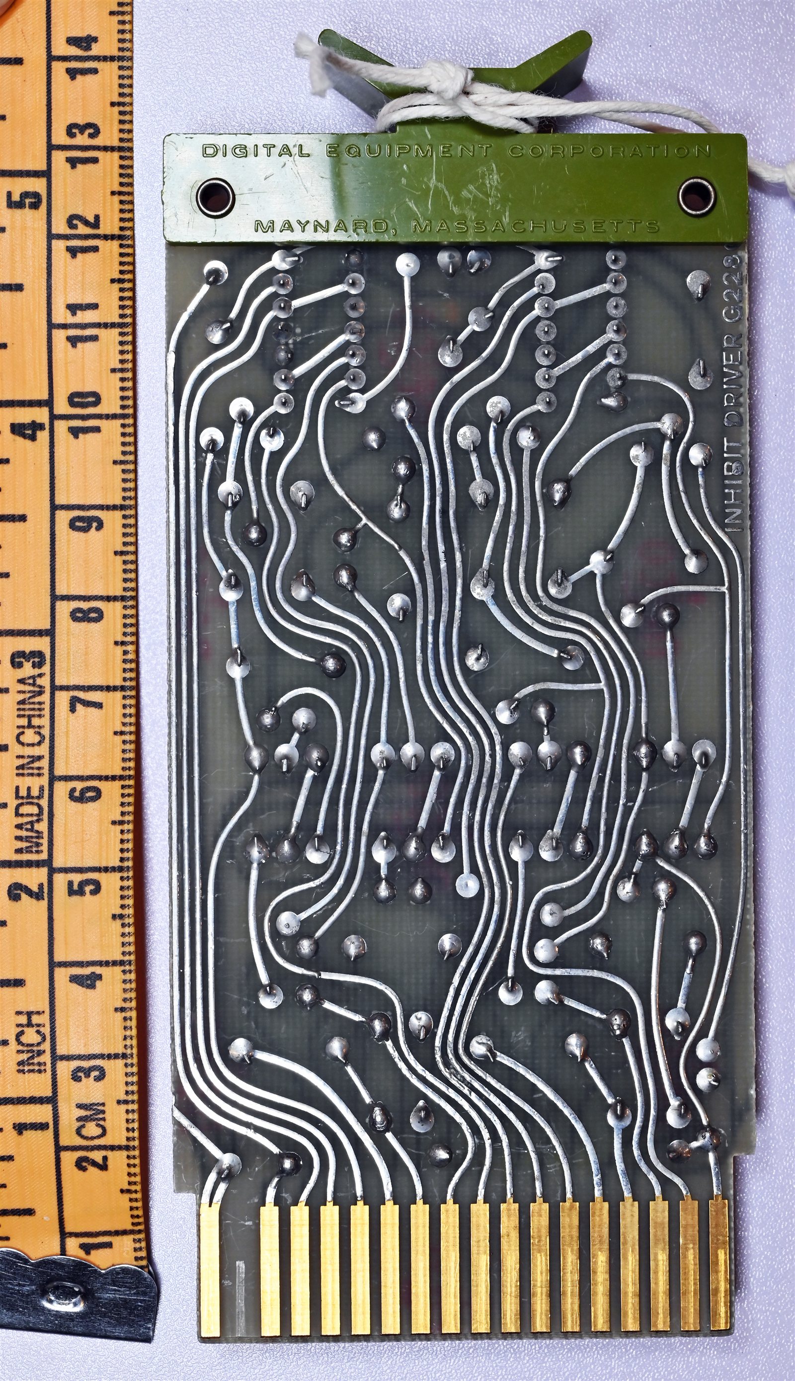
A pile of cards is not a computer; every module’s contacts have to be joined to the right contacts on the others so signals flow in the pattern the design demands. DEC made those connections in the backplane — the structure at the back of the card cage into which the module sockets are mounted. On the reverse of the backplane, behind each socket, stood rows of small square metal posts, one per contact, and the wiring between modules was made by wire-wrapping: a length of fine wire (the M-series machines used thin 30-gauge wire) wound tightly, many turns, around a post, the post’s sharp corners biting into the wire to form a gas-tight, solderless connection both reliable and easy to change. A wrapping machine, following a wire list generated from the design, made the hundreds of point-to-point connections semi-automatically. The result is the machine’s nervous system: a dense thicket of wires on the back of the backplane, each joining a pin on one module to a pin on another, realizing in copper the schematic of the processor.
So the recipe for a PDP-8/I processor is a recipe rather than a single artifact: take roughly a hundred small flip-chip cards, each a few TTL chips’ worth of logic; plug them into the sockets of a card cage; and on the back, wire-wrap the backplane to tie them into the twelve-bit machine. Pull a card and you hold a piece of the processor in your hand — a few gates of the accumulator, say, or part of the instruction decoder; slide it back and the machine is whole again. This modules-in-a-backplane construction is how essentially every DEC computer of the era was built, and it is the form the architecture of Volumes 4 and 5 actually took: registers, adders, and control logic parcelled out across a wall of little cards, stitched together by wrapped wire.
6.6 Packaging, power, and the front panel hardware
Memory stack and module rows still need a body to live in. The machine was housed in a cabinet — commonly a tall rack — with the processor and memory mounted on a slide-out framework. To service it you drew the assembly forward out of the cabinet, and the logic could be opened like a book: hinged sections swung apart to expose the wire-wrapped backplanes on their inner faces, so a technician could reach the wiring just described, probe a pin, or rewrap a connection. It was built to be opened and repaired, not sealed away.
All of that logic ran on direct-current power, and supplying it was a substantial part of the machine. TTL wants a steady, well-regulated +5 volts, and the core memory’s drivers wanted their own voltages besides; the power supply took the building’s alternating-current mains and turned it into those stiff DC rails, delivering the considerable current a hundred-odd chip-laden cards and a set of core drivers demand. It was correspondingly bulky and heavy — a transformer, rectifiers, and regulation — and as much a part of the physical machine as the logic it fed. With current comes heat: a wall of TTL dissipates real power as warmth, and the cabinet was cooled by forced air, fans drawing a draught across the module rows to keep the silicon within its limits. This is the unglamorous half of why the machine was the size it was: a good fraction of the box goes not to logic but to powering and cooling the logic.
The one part the operator actually faced was the front panel — the famous wall of switches and lamps across the front of the PDP-8/I, suspended at the front of the slide-out assembly. As hardware, the panel is two things. First, a bank of toggle switches: a horizontal row of twelve, the Switch Register met in Volume 4, by which a human sets a twelve-bit value by hand, plus a cluster of control switches (load, deposit, examine, start, and the rest). Second, a field of indicator lamps — small incandescent bulbs behind a legended panel — that display, bit by bit, the live contents of the machine’s key registers: the program counter, the memory address and buffer, the accumulator and link, and the major state of the processor. The lamps are wired straight to the flip-flops they report, so they glow in real time as the machine runs; the switches feed straight into the logic. The panel is, in hardware terms, simply the machine’s registers brought out to a row of switches and a grid of light bulbs where a person can reach them. Using it — toggling a bootstrap into memory a word at a time, single-stepping a program, reading a result out of the lamps — is the craft Volume 7 is devoted to. Here it is enough to see the panel for what it physically is: the operator’s interface, hardware like the rest, the one face of the box built for human hands and eyes.
6.7 What’s physically inside: a tour of the machine
Put it all together and walk through the real object, front to back, the way you would if you slid a PDP-8/I out of its cabinet and opened it up.
At the front is the panel: the row of twelve toggle switches and the control switches beside them, and around them the grid of indicator lamps, each bulb wired to a flip-flop somewhere inside. This is the only part made for a person, and through it everything else is reached.
Behind the panel are the rows of modules — the card cage, full of small flip-chip boards standing on edge in their sockets, perhaps a hundred of them, each carrying a few TTL chips. Spread across those cards is the entire processor of Volumes 4 and 5: the accumulator and its link, the program counter, the memory address and buffer registers, the adder, the instruction decoder, the timing and control logic. Among them, in its own inch-thick aluminum module, sits the core stack — twelve woven planes of 4,096 ferrite rings, threaded with their X, Y, sense, and inhibit wires, holding the 4,096 twelve-bit words of the machine’s one field, their driver and sense-amplifier cards clustered around them. This little box is the memory; everything the program is and everything it touches lives as patterns of magnetization in those rings.
At the back of the cage is the backplane, and on its rear face the dense mat of wrapped wire — the hundreds of post-to-post connections that turn the pile of cards into a coherent twelve-bit computer. This is the wiring you could swing open like a book and probe. Filling out the cabinet, away from the logic, is the power supply with its heavy transformer and regulators turning mains into the +5-volt rails, and the fans pulling cooling air across it all.
That is the PDP-8/I as a physical fact: a face of switches and lamps; a cage of small TTL cards realizing the processor; a woven stack of iron rings holding the memory; a wire-wrapped backplane tying it together; and a power supply and fans keeping it fed and cool. The architecture of the earlier volumes — twelve bits to a word, one accumulator, a field of 4K — is what this object was arranged to be. When Jeff’s replica lights its panel and steps its program counter, it is conjuring this machine: not an abstraction, but a real arrangement of magnetism, silicon, copper, and sheet metal that a person in 1968 could roll out of a rack and fix with their hands. The next volume puts those hands on the front panel and learns to drive it.
Sources
- Doug Jones, “A Type 184A Core Memory Module” and the PDP-8 core-memory pages (University of Iowa). Detailed first-hand description of the PDP-8/I’s 12-plane core stack, the 64×64 (4,096-core) planes, the four wires through each core (X, Y, sense diagonal, inhibit parallel to Y), the coincident-current half-select scheme, the diode-balun selection matrices, the core dimensions (~0.035 in diameter), and the 1.5-microsecond read-and-restore cycle time. https://homepage.cs.uiowa.edu/~jones/core/pdp8/
- Doug Jones, “DEC PDP-8 Models and Options” (University of Iowa). Confirms the PDP-8/I as the first TTL PDP-8; the M-series flip-chip modules (TTL on +5 V, double-sided 36-contact edge connectors versus the older 18-contact single-sided cards, ~4 SSI chips per card); 30-gauge wire-wrapped backplanes; the Ferroxcube core supplier; the ~6-inch aluminum core box built from rigid 5×5-inch boards; the 3-microsecond add time; and the memory-quality problems that led some early machines to run a slower cycle. https://homepage.divms.uiowa.edu/~jones/pdp8/models/
- Wikipedia, “Magnetic-core memory.” Corroborates the physics: ferrite toroids magnetized clockwise/counter-clockwise to store a bit; the square hysteresis loop giving bistability and a select threshold; coincident-current X/Y selection by two half-currents summing at the chosen core; sense and inhibit wires; destructive readout and the mandatory read-rewrite cycle; the access-time-versus-cycle-time distinction; and core’s non-volatility. https://en.wikipedia.org/wiki/Magnetic-core_memory
- Wikipedia, “PDP-8.” Confirms the twelve-bit word and 4K (4,096-word) field organized as twelve bit-planes, the integrated-circuit (TTL) construction of the 8/I, flip-chip modules on a wire-wrapped backplane, and the front-panel switch register and indicator lamps as the operator interface. https://en.wikipedia.org/wiki/PDP-8
- PDP-8/I & PDP-8/L Small Computer Handbook / maintenance manuals (Digital Equipment Corporation), via bitsavers.org. DEC’s own documentation of the core-memory subsystem, the M-series module logic, backplane wiring, power, and the front-panel hardware. http://www.bitsavers.org/pdf/dec/pdp8/
- pdp8online.com, “PDP-8/I Front Panel,” and dustyoldcomputers.com PDP-8/I pages. Photographs and descriptions of the slide-out chassis that opens like a book to expose the wire-wrapped backplanes, the front panel of switches and indicator lamps, and the physical layout of the machine. http://www.pdp8online.com/pdp8i/pics/pdp8i_frontpanel.shtml · http://dustyoldcomputers.com/pdp8/pdp8i/index.html
- Figure (core plane): “Magnetic-core memory 8k × 12 bit H-212 — close up,” photograph by José Luis Briz Velasco at the Museo de Informática Histórica (UNIZAR), via Wikimedia Commons, licensed CC BY-SA 4.0 — a twelve-bit-word core memory representative of the PDP-8/I’s. https://commons.wikimedia.org/wiki/File:Museo_de_Inform%C3%A1tica_Hist%C3%B3rica_(MIH)_%E2%80%93_UNIZAR_%E2%80%93_Magnetic-core_memory_8k_x_12_bit_H-212_%E2%80%93_close_up.jpg
- Figure (flip-chip module): “DEC Flip Chip - back,” photograph by Jud McCranie, via Wikimedia Commons, licensed CC BY-SA 4.0 — a DEC flip-chip module showing the printed-circuit card and its edge-connector contacts. https://commons.wikimedia.org/wiki/File:DEC_Flip_Chip_-_back.jpg
_%E2%80%93_UNIZAR_%E2%80%93_Magnetic-core_memory_8k_x_12_bit_H-212_%E2%80%93_close_up.jpg)
Comments (0)